

Actual and future requirements on laser processing for highefficiency crystalline solar cells


Introduction:
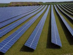
It is about 15 years ago when the production of crystalline Silicon (c-Si) solar cells and thin film modules moved from small quantities to a mass production scale. A review of the evolution in process technology of this young industry reveals laser processing to play an
ambiguous role. InnoLas, who started its developments in solar cell technology already in 1999 and was the pioneer in laser processing since the beginning of the photovoltaic (PV) industry, was able to successfully install the first laser process machines for the production of c-Si solar cells in 2003.
The first process step suitable for laser processing was via drilling for Metal/Emitter Wrap Through (MWT/EWT) solar cells, which however could only reach a limited market volume as MWT/EWT never took off to become a mainstream solar cell technology.
The second one was the laser edge isolation (LEI) process, which became the leading technology to isolate the front and rear sides of the industrial standard c-Si solar cells. Only a few years later it was gradually replaced by a single sided wet chemical etching process yielding higher cell efficiencies.
In parallel to the laser processes for c-Si solar cells, laser scribing technologies (P1, P2, and P3 patterning) for thin film solar modules were developed and introduced to the market. Surely the laser scribing processes were a very successful and enabling technology for thin film modules, however, always limited by the smaller market share of the thin film compared to the c-Si technology.
From 2005 on InnoLas started to work on new technologies for standard c-Si solar cells like laser-doped selective emitter (LDSE) and laser contact opening (LCO). LDSE became another short hype around the year 2010 and was superseded by a continuously optimized printing technology rendering the benefits of a selective emitter unnecessary.
So we saw a lot of up and downs for laser processing in the PV industry over more than a decade, and today it looks like LCO is about to establish itself as a mainstream process in the manufacturing of industrial standard solar cells. The reason can easily be found in the international technology roadmap for PV (ITRPV).
According to the ITRPV the passivated emitter rear cell (PERC) is becoming a dominating technology in the area of c-Si solar cells during this and the next two years wherein LCO is a necessary process step. So far there is no suitable metal paste to be fired through the deposited passivation layer.
Consequently, laser ablation is the most cost effective method to locally open the area to be contacted by the fully covering Aluminum paste on the rear side of the solar cell. Going a little bit further in the ITRPV to next generation technologies we find the LCO process not only on the rear side. The front side dielectric (usually SiN) can be opened by lasers as well to enable direct plating on Silicon (PoSi).
As long as the Cu printing technology is lacking the ability to provide the inevitable diffusion barrier between Cu and the Si wafer, the PoSi technology is the main road to replace the costly Ag metal grid with the much cheaper Cu, since it can plate a stack of Ni, Cu, and Ag or Sn, which is required to embed the harmful Cu in between a diffusion inhibiting and a surface passivating layer.
And going one more step further in the ITRPV we find again a very promising LCO process, namely in the technology of interdigitated back contact (IBC) solar cells, which are predicted to enable the jump over 23% efficiency.
Requirements on laser machines for mass production A laser source, a scanner, some optical components, and a controlled x/y stage make a laser machine. Everything is available off the shelf and it looks like it can be built by anyone. This fundamental misunderstanding often led to frustration and jeopardized thesuccess of laser machines as a highly cost effective and even enabling technology in the PV industry.
A variety of unavoidable influencing factors from outside, such as e.g. temperature variations, vibrations, pollution, amongst others, lead to degradation of the laser beam quality and alignment and must be eliminated by proper countermeasures in the machine design. Insufficient exhaust causes a so-called clouding effect, which is a cloud of dust generated from removed material during a laser ablation process.
And laser sources exhibit a certain power degradation over time by nature, which must be compensated for. InnoLas looks back onto 20 years of experience in building machines for laser applications in the PV, electronics, semiconductor, and printed circuit board industries.
Over this time period InnoLas continuously developed its unique platform strategy to the point of a standardized machine base with all fundamental features of a laser production machine, which can be equipped with the applications-specific laser source and optics.
A worldwide install base of more than 350 machines based on not more than 4 basic tool platforms allowed a holistic optimization of these platforms. High speed galvanometer scanners, automatic vision alignment and machine calibration systems, which have been integrated repeatedly by InnoLas, assure a very high accuracy and stability in a 24/7 production environment as well as extremely high throughputs up to 3600 wafers per hour for various process applications.
As an acknowledgement for its evolving laser system technology, InnoLas was awarded the 2014 Solar Award Winner at the EU PVSEC trade show for its LCO process and machine solution. The reason for winning the Award was that InnoLas developed the fastest laser process with an outstanding Cost of Ownership (CoO) for the PERC technology, which opens the window to affordable high efficiency solar cells. Other than wet chemical, CVD, or printing processes, the laser processing is almost free from consumable costs.
Main contributors to CoO are capital investment per throughput,
maintenance cost, and operating cost. Therefore the task of the laser equipment provider is to design a system, which is based on a standardized and proven industrial platform such as InnoLas ILS-TT, and avoids any fancy and unnecessary optical features.
A few examples: nanosecond laser sources are cheaper than picosecond laser sources and can be superior in performance for LCO through their ability to create a melting zone at the Si surface. They can achieve the highest throughput through very high repetition rates and can provide enough power for supplying two process heads with one laser source, presuming the right laser source is chosen by the machine vendor.
Maintenance and spare part cost can be minimized by choosing a laser source with a diode lifetime greater than 40.000 hours and with no need for an external cooling system. Stationary processing with conventional scanner technology is by far more reliable and cost effective than so called on-the-fly processing with polygon scanners.
System uptime can be optimized by automatic calibration routines, which avoid stopping the production machine for mechanical adjustments. There is still a variety of system parameters, which contribute to an optimized laser production tool with the lowest cost of ownership in the market, as provided by InnoLas.
Processes and tool solutions for PERC From a process integration point of view, a line pattern represents the easiest and most common way to implement LCO for PERC. Today, the standard process is a line opening with 30-50μm wide lines, and a line-to-line distance of 1 mm.
Such a relatively wide opening in the passivation layer presents a good interface for the subsequent contact formation during the co-firing of the screen printed metal layer. The larger the local surface opening is the faster and more homogeneously the Aluminum-Silicon alloying process can start.
This has a direct influence on the formation of the local back surface field (BSF) during the alloying and affects the final Voc. On the other hand, from the perspective of the PERC solar cell design, the wide opening lines restrict the final cell efficiency, because more open area reduces the passivated area leading to lower current (Isc) and voltage (Voc).
In order to extract the whole electrical current from a typical PERC solar cell the required cross-section-equivalent opening ratio is 1% ± 0.2%. For a line opening pattern, the opening ratio is in the range of 3% to 6%. Increasing of the line to line distance would help to reduce the opening ratio and therefore increase the Voc and Isc, but the series resistance (Rs) and consequently the fill factor (FF) of the solar cell will suffer. Especially for high ohmic wafer material the effect can become dramatic.
It is sometimes believed that an optimum contact design combining the opposing requirements of opening ratio and series resistance would be a dot pattern with equidistant dot-to-dot spacing. The drawback of this design, however, is that contact formation during the co-firing process is made difficult.
While a line represents a onedimensional opening which allows for compensating local inhomogeneity of the local BSF (e.g. voids), every dot is a single event which contributes significantly to the final cell performance. If the contact formation process is not applied perfectly, some of the dots may fail and the solar cell significantly suffers from loss in Voc and Rs/FF, despite an almost optimal opening ratio of 1% to 1.6%. As of today, there are not many users known who could manage this tricky process in mass production.
A loophole from the described restrictions of the line opening and the dot opening designs is given by the so-called dash pattern. Such a dashed line pattern consists of scattered lines with an asymmetric relation of the length of the dash and the gap in between two dashes.
The ratio between dash and gap is determined by the aluminum paste and the firing conditions used, and allows for a wide range of parameter combinations. Consequently, the complexity of finding the optimized dash pattern is higher than for a line or dot pattern, but is rewarded by an excellent PERC solar cell performance.
The contact formation behavior is comparable to a line pattern and an opening ratio of 1.4% – 3% is achieved, which is close to a dot pattern. Additionally, if the rear side bus bar pads, which do not contribute to the electrical contact and BSF formation, are kept free from the LCO process the opening ratio can be optimized further.
Considering the various factors contributing to the performance of the rear side of PERC solar cells, it becomes obvious that the future direction of optimization will be to manage the increasing complexity of the dash pattern design, leading to a layout with changing dash and gap lengths across the wafer. This is related to connected upstream and downstream processes in the production line and will become necessary to achieve the optimum current yield for the solar cell rear side.
Although the performance of PERC solar cells today is often limited by their front side design, it is clear that only with this complexity of the rear contact design, PERC solar cells will reach their efficiency optimum in the future.
There are not only a few technologists, who believe that optimization of the PERC solar cell rear side comes along with a revival of the LDSE technology or the implementation of new metallization schemes such as PoSi in order to overcome the
actual limitations of the front side.
From a laser machine point of view the line opening process is a relatively simple approach. The laser is switched on and the laser beam moves from the desired starting point of the line to its ending point, where the laser is switched off. Repeating this procedure over the entire wafer surface leads to the specified line pattern. InnoLas has developed this process already 10 years ago and has been continuously improving it along with equipment for highest throughput and precision as unique in the industry.
Scanning speeds up to 25m/s using a robust and well-developed galvanometer scanner technology together with InnoLas´ ILS TT tool platform supports customer requirements on throughput of up to 3600 wafers per hour either as fully automated stand-alone or inline solution.
Guided by its outstanding know how in the more difficult laser processing of IBC solar cell architectures, about two years ago InnoLas was able to introduce a high speed dash pattern technology to the market, utilizing its outstanding scanner technology and control software to run highly complex dash patterns with the same high scanning speed as a simple line pattern without losing accuracy.
In order to meet the requirements of the more and more complex dash pattern, the design of the layout has to be done with CAD software. InnoLas’ novel software directly converts the CAD layout into a machine compatible script and recipe package, which optionally can be downloaded via MES from an external workstation directly to the production machine.
Meanwhile, a production capacity of over 3 GW of PERC solar cells is rolled out with InnoLas’ high speed dash
pattern technology.
Future trends in laser processing for the PV industry There is no more doubt, that PERC technology is becoming a mainstream in standard industrial solar cell production. The question arising is “what is next?” A good candidate to make the race to become a new standard process is Cu metallization to replace the costly Ag printing, which accounts for almost 50% of the solar cell production cost.
RENA Technologies, the pioneer in the PV industry for wet chemical processing equipment, and chemical vendor MacDermid together with InnoLas developed an electroplating process to directly deposit a stack of Ni, Cu, and Ag on laser opened areas of the Si substrate (Plating on Silicon, PoSi). The technology package developed by the three partners comprises of a front side LCO process followed by subsequent PoSiand post annealing processes, which can be directly integrated into existing production
lines as an upgrade.
With this package for the first time a proven industrial solution is being offered where the formerly well known adhesion problems of the metal stack after soldering have been solved. The key to this technology is the choice of the right laser process together with a perfect adaption of the plating method and chemistry.
In contrast to the rear side LCO process for PERC, the front side LCO process for PoSi does not allow any melting of the textured Si surface and damage to the sensitive junction, while the passivation layer must be removed thoroughly with no residues hindering the onset of the metal growth process.
The technology developed by RENA, MacDermid, and InnoLas works for standard as well as PERC solar cells and does not require any changes to the standard module assembly and soldering process. Module reliability tests have already been passed successfully with excellent results and no degradation of the module performance after heat cycling testing.
Laser fired contacts (LFC) are commonly dealt as next generation PERC technology, whereby the Al printing and co-firing steps are substituted by a layup of an Al foil directly onto the passivated rear side, which is locally fired and subsequently cut out by lasers, all
being processed within one single laser equipment.
A significant cost reduction compared to the actual LCO, Al printing, and co-firing processes will be enabled. As the exclusive partner of the patent owning technology developer Fraunhofer ISE, InnoLas has already developed the required laser processes as well as prototype equipment for the foil layup. Challenges still to be solved are on the industrial maturity of the technology and passing
the module reliability testing.
IBC or IBC-related solar cell concepts are starting to become more and more relevant for companies, who managed to exceed a certain level of cell efficiency performance. IBC cell architecture represents a more revolutionary step in the efficiency roadmap than evolutionary steps like PERC, PoSi, or n-type bifacial cells.
There is a significant gap between the requirements of e.g. a standard production line with PERC upgrade and a fully blown IBC production line in terms of process stability, reliability, and precision, and the equipment for IBC production must fulfill specifications close to semiconductor standards. E.g. an alignment accuracy of down to ±10 μm with an absolute precision of ± 5 μm in 24/7 production must be achieved.
The complete control of all functions of a leading-edge ultra-short pulse laser source is only one of the required enhanced features next to an integrated analytics for inline characterization of the laser process result to close the feedback loop with the machine and to assure that the process result is always within a tight process window.
More than thirty machines meeting these challenging requirements have already been installed by InnoLas for industrial production of IBC. The most obvious application for laser processes on IBC cell architectures is again an LCO process substituting the cost-intensive photo-lithography and wet etching processes, which were needed to create the metal pattern of the interdigitated fingers. Besides LCO,
there are a couple of other possible applications for laser processing on IBC, which are still under investigation.
Summary –
The historical role of laser processing for the fabrication of industrial standard c-Si solar cells is ambiguous. Several applications for lasers such as via drilling, laser edge isolation, laser doped selective emitters emerged and vanished. Laser contact opening is about to establish itself as a mainstream technology in the PV industry and is indispensable from PERC solar cells.
State-of-the-art laser machines for mass production must dispose of automatic routines to compensate for misalignments and laser degradations over time, and must be able to run sophisticated patterns at a very high speed and throughput in order to achieve optimum efficiency at affordable cost. In future, the laser contact opening will play an increasingly important role, e.g. for electroplated Cu metallization or IBC solar cells.
Authors: Rico Böhme, Ernst Hartmannsgruber (InnoLas Solutions GmbH)