


Plasma passivation process to cut silicon cell costs


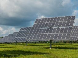
Scientists in Saudi Arabia have developed a new passivation process for n-type silicon solar cells, which they say could offer a simpler, lower-cost alternative to current processes used in manufacturing. The group fabricated wafers using this process with promising results, and now plans to integrate the process into a full silicon cell.
Scientists at the King Abdullah University of Science and Technology (KAUST) in Saudi Arabia discovered a new process utilizing carbon dioxide in plasma, which they claim could offer several improvements over current processes used to passivate silicon solar cells.
Passivating contacts are important in cell production, to reduce recombination at the surface and thus improve efficiency. The processes currently used for depositing this layer, however, are complex and require high temperatures. “The problems with existing methods challenged us to find a more simple and practical process,” said KAUST Ph.D. student Areej Alzahrani.
The group discovered that exposing the silicon to carbon dioxide in plasma allowed them to carefully control the deposition of a silicon oxide layer. They were able to grow a layer less than two nanometers thick onto an n-type silicon wafer, and then deposit p-type polysilicon contacts on top. KAUST says that by integrating both of these steps in one chamber, cell manufacturers could significantly reduce their costs.
Encouraging results
The process is described in the paper In Situ Plasma-Grown Silicon Oxide for Polysilicon Passivating Contacts, published in Advanced Materials Interfaces.
Popular content
Wafers fabricated using this process were found to have excellent passivation properties, with implied open-circuit voltage higher than 700 millivolts, and contact resistance as low as 0.02 ohms per square centimeter. The group also found that, after thermal annealing at 1000 degrees Celsius, the wafers it fabricated demonstrated better structural integrity and stability at high temperatures.
KAUST says that having demonstrated the technique, it now plans to fabricate full solar cells using the technique, allowing it to further evaluate the commercial potential. “A first step will be to integrate this process into a complete and working solar cell,” says Stefaan De Wolf, Associate professor at KAUST, “while also exploring improved light-capturing designs.”